Our portfolio encompasses diverse designs such as bandgap references, Sigma-Delta modulators, ADCs, LDOs, OpAmps, UVLs, and more.
Extensive Experience in Analog and Mixed Signal IC Design
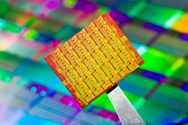
Our analog engineers boast extensive expertise in analog and mixed-signal IC design across a range of technologies, spanning from 350nm and 180nm HV planar nodes to 65nm and SOI technologies.
Capabilities
In our team, we offer a complete set of advanced features and technologies in IC design and simulation:
Specification writing and feasibility analysis
Circuit design and simulation
Analog and custom digital layout design
Physical verification of the design (DRC, LVS, ERC, DFM)
Layout parasitic extraction and post-layout simulation
Verilog A and Verilog AMS model development
Support for production and manufacturing
Engineering and manufacturing documentation
Technologies and tools
In our team, we offer a complete set of advanced features and technologies in IC design and simulation:
High Voltage XFAB 350 nm and 180 nm nodes
TSMC 180 nm, Global foundries
SPICE simulation (Eldo, Spectre, HSpice)
Verilog A, Verilog AMS
Monte Carlo, PVT analysis, parametric extractions
Cadence/ Synopsys/ Siemens
Complex custom layout
Mixed-Signal design validation
Simulation batching and automatic report generation
Intellectual Property (IP) Cores
Verilog A, Verilog AMS
Monte Carlo, PVT analysis, parametric extractions
Cadence/ Synopsys/ Siemens
Complex custom layout
Mixed-Signal design validation
Simulation batching and automatic report generation
Intellectual Property (IP) Cores
Sample project
High-voltage isolated analog buffer for an IC to be used in commercial automotive and energy applications. Currently under final testing by the customer (call for details). The design IP included Mixed-Signal blocks on 350 nm high-voltage CMOS commercial process:
Single-ended OpAmps and bias circuits, biphasic oscillator and latched comparator for modulator
Demodulation active RC 2nd order low-pass filter
Final delivery of schematic level design, full corner verification (on agreed specs), final layout, DRC and LVS checks, full chip padframe design and extra circuitry for analog and digital post-fab testing.